
As global demand for faster data transmission, advanced optical communication, and high-speed computing continues to rise, integrated photonics has become one of the fastest-growing sectors in modern technology. Among the key materials driving innovation in this field, Lithium Niobate Wafers are gaining significant attention due to their exceptional electro-optic, nonlinear optical, and piezoelectric properties.
Traditionally used in RF filters and optical modulators, Lithium Niobate Wafers are now finding expanding applications in integrated photonics, enabling next-generation devices with higher speed, lower power consumption, and improved signal performance. As a professional wafer supplier, CQT provides high-quality wafer solutions that support the growing demands of photonic integration technologies.
Integrated photonics refers to the integration of multiple optical functions onto a single chip, similar to how electronic integrated circuits combine multiple electronic components.
Photonic integrated circuits (PICs) can perform functions such as:
· Optical signal transmission
· Data modulation
· Signal filtering
· Frequency conversion
· Optical switching
· Sensing and detection
Compared with traditional electronic systems, integrated photonics offers:
· Higher bandwidth
· Faster data transfer
· Lower latency
· Reduced power consumption
· Smaller device size
This technology is becoming increasingly important in telecommunications, artificial intelligence, cloud computing, and quantum technologies.
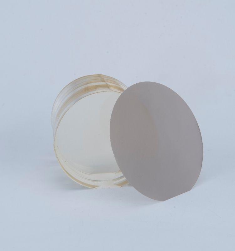
Lithium niobate is widely recognized as one of the most versatile optical materials available today.
One of the biggest advantages of Lithium Niobate Wafers is their strong electro-optic effect.
This allows the material to rapidly change its optical properties when an electric field is applied.
Benefits include:
· Ultra-fast optical modulation
· High-frequency signal control
· Low optical loss
· Excellent signal stability
These properties are critical for high-speed optical communication systems.
Lithium niobate also exhibits excellent nonlinear optical behavior, making it suitable for advanced photonic functions such as:
· Frequency conversion
· Wavelength generation
· Optical amplification
· Quantum photonics applications
This versatility has expanded the role of Lithium Niobate Wafers far beyond traditional telecom applications.
One of the largest growth areas for lithium niobate photonics is optical communication.
Optical modulators are essential for converting electrical signals into optical signals for fiber-optic networks.
Lithium Niobate Wafers enable modulators with:
· Extremely high bandwidth
· Low insertion loss
· Fast response speed
· Stable long-distance signal transmission
As data centers and 5G infrastructure continue expanding, demand for high-performance optical modulators is increasing rapidly.
Modern data centers are moving toward co-packaged optical systems that integrate photonic and electronic components more closely.
Lithium niobate photonic devices help support:
· Faster server communication
· Reduced energy consumption
· Improved signal integrity
· Higher network capacity
CQT provides precision-engineered Lithium Niobate Wafers suitable for advanced optical device manufacturing.
One of the most important recent developments is Lithium Niobate on Insulator technology.
LNOI combines thin-film lithium niobate with insulating substrates to create highly integrated photonic platforms.
Advantages include:
· Compact device structures
· Improved optical confinement
· Lower power consumption
· Enhanced modulation efficiency
LNOI technology has significantly accelerated the adoption of integrated lithium niobate photonics.
LNOI enables smaller and more efficient photonic components, supporting:
· Compact transceivers
· Integrated optical chips
· High-density photonic circuits
· Portable optical systems
Miniaturization is becoming increasingly important in cloud computing and mobile communication infrastructure.
Quantum technology is another area driving interest in Lithium Niobate Wafers.
Lithium niobate can support advanced quantum optical functions such as:
· Photon generation
· Quantum frequency conversion
· Entangled photon manipulation
These capabilities are important for future secure communication systems.
Researchers are exploring lithium niobate photonic platforms for scalable quantum computing architectures due to their low optical loss and excellent modulation properties.
As quantum technologies evolve, demand for high-quality wafer materials is expected to grow significantly.
Integrated photonics is also transforming sensing technologies.
Lithium niobate photonic devices are increasingly used in LiDAR systems for:
· Autonomous vehicles
· Robotics
· Industrial automation
· Environmental mapping
The material’s fast optical modulation capability supports high-resolution sensing performance.
Lithium Niobate Wafers are also used in advanced optical sensors for:
· Medical diagnostics
· Environmental monitoring
· Industrial process control
· Aerospace systems
Their high sensitivity and stable optical behavior make them ideal for precision sensing applications.
Several factors make lithium niobate highly competitive in integrated photonics.
Lithium niobate supports extremely high-frequency optical modulation, making it ideal for next-generation communication systems.
Efficient signal transmission helps reduce power consumption and improve overall system performance.
High-quality Lithium Niobate Wafers manufactured by CQT provide:
· Stable crystal quality
· Uniform thickness control
· Low defect density
· Consistent optical performance
Reliable wafer quality is essential for advanced photonic device fabrication.
The future of integrated photonics is closely linked to the continued advancement of lithium niobate technologies.
Key growth areas include:
· AI data center infrastructure
· 6G communication systems
· Quantum communication networks
· High-speed optical interconnects
· Advanced sensing platforms
As photonic integration becomes more important across multiple industries, Lithium Niobate Wafers will continue playing a central role in technological innovation.
The emerging uses of Lithium Niobate Wafers in integrated photonics are transforming modern optical communication, sensing, and quantum technologies. With outstanding electro-optic performance, low optical loss, and strong nonlinear properties, lithium niobate has become one of the most promising materials for next-generation photonic integrated circuits.
As demand for faster and more efficient optical systems continues to grow, CQT remains committed to supplying high-quality Lithium Niobate Wafers that support advanced photonic innovation across global technology markets.
Previous: Why Quartz Glass Substrates Are Used in High-Temperature Optical Systems
Next: None.
Copyright:@2020-2021

Comments Please sign in or sign up to post.
0
0 of 500 characters used